
Tracking Down and Resolving Emissions From a Power Supply Chip (On-Semi NCP81239)
Troubleshooting a radiated emission issue on one of our USB Type-C PD designs resulted in a surprising discovery and an unconventional solution
We recently needed to dig deep into a 60W power delivery design for one of our clients. It showed radiated emissions in excess of FCC class B target and we needed to get to the bottom of it. The pre-compliance work had already been done at E3 in Grand Rapids, so though we weren't present for the testing we had access to the data. At first it looked like a straightforward need to add a common mode choke to the input. Further investigation on the bench with nearfield probes showed a very sharp spur at 49MHz and several harmonics coming directly from the NCP81239 buck boost chip we use as a power supply.
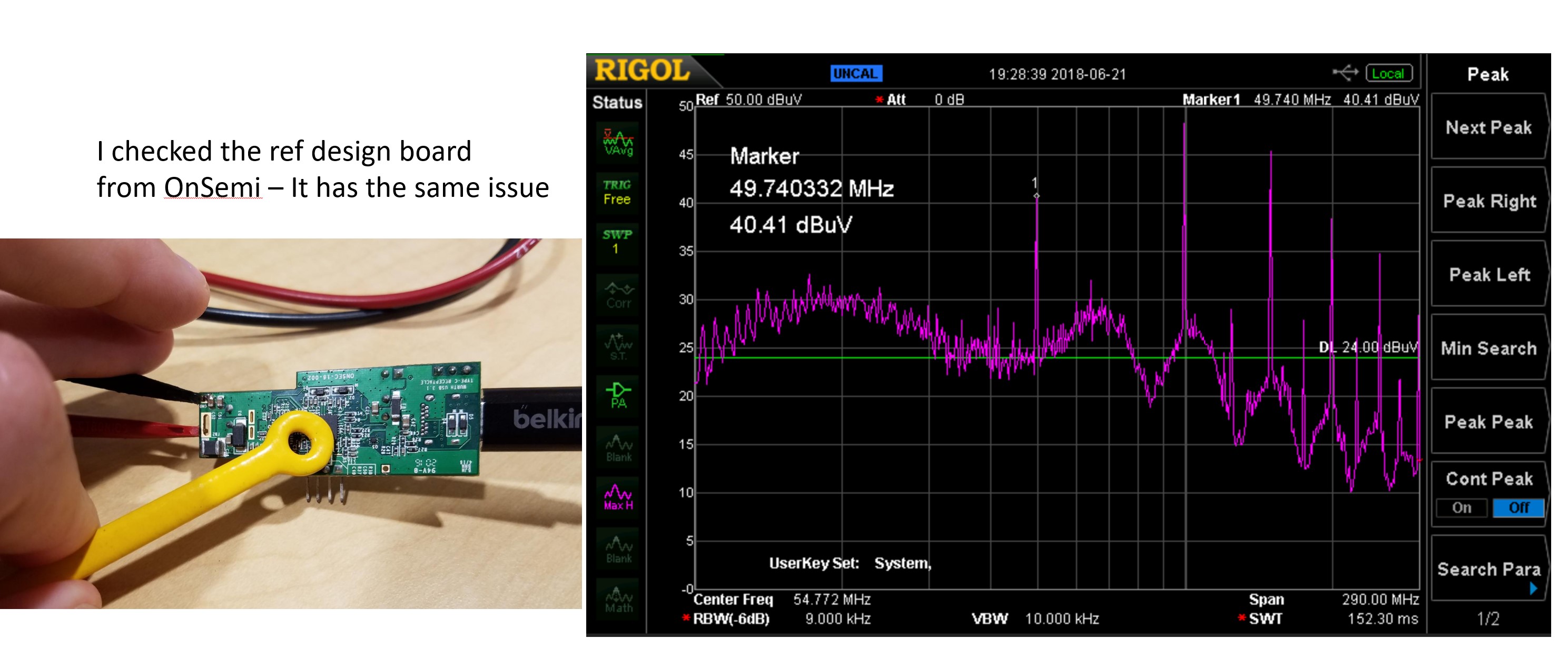 Near-field emissions from NCP81239 on On-Semi reference design board
This supply is tailor-made for USB type-C power delivery because the output voltage is controllable via I2C. Since PD requires adjustable output from 5 to 20V the I2C interface provides a lot of flexibility.
So back to the 49MHz spur – It’s unusual to see this kind of frequency coming from a power supply chip. It’s usually the kind of emission you see from a micro or clock generator. The characteristics of the emission indicate that the source has a 49MHz fundamental frequency, that the waveform is asymmetric, and the rise time is probably > 3ns.
How can I tell that?
- The fundamental is 49MHz because it's the first spur to appear in the spectrum
- I know the waveform is not pure square wave or trapezoidal wave because the even harmonics are present
- The rise time of the edges governs the point at which the intensity starts to roll off - right around 100MHz which indicates a 3ns RT
Normally in a power supply you look for high megahertz noise caused by ringing at the switch-node or in the gate drives. All these looked clean.
I contacted On-Semi to see if there was some hidden clock feature that's not mentioned in the datasheet. They pointed me to their reference design and told me I must have done something wrong. Fortunately, I have the reference design board. It has the exact same emission. Since the signal is not being generated by FET switching, it indicates that it is coming from inside the chip.
I thought I would take a look at the decoupling cap for the chip. For the chip internal logic to be driving something that hard it needs a low impedance power source - i.e., the decoupling cap. I looked at the voltage across the cap and sure enough, there was the asymmetric 49MHz waveform.
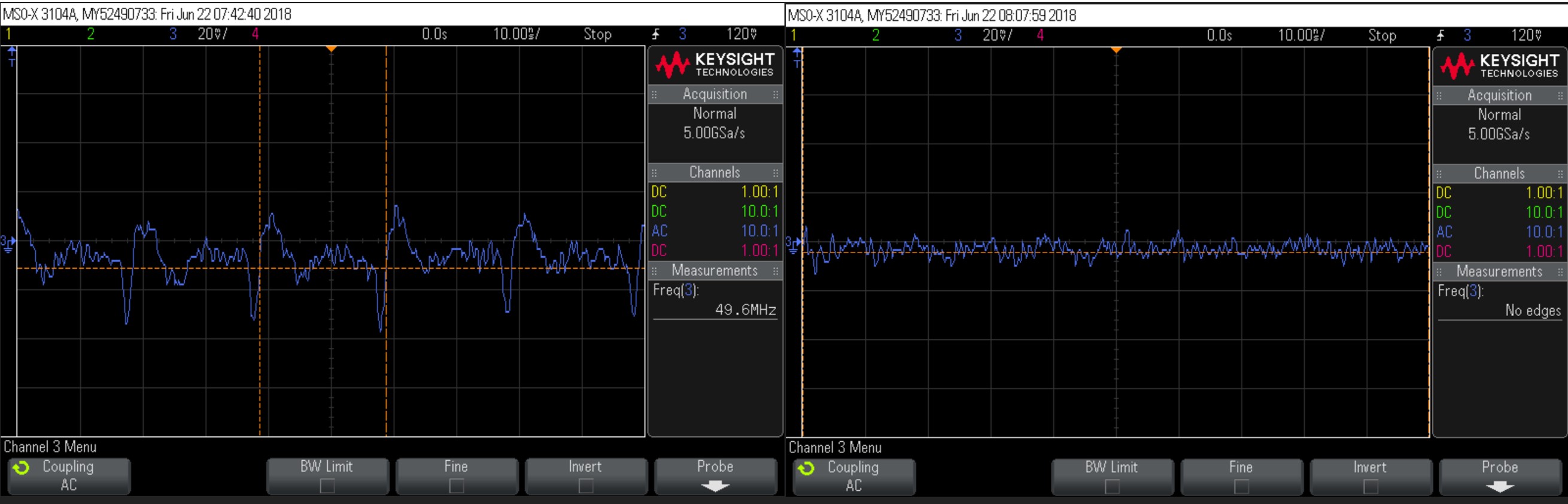 Voltage across NCP81239 Vcc decoupling capacitor before (left) and after fix (right)
Next step was to try limiting the bandwidth of that supply. I placed a ferrite bead in series with the decoupling cap and voila! - no more noise across the cap and no more nearfield emissions from the chip. Impedance of the cap was still low enough at lower frequencies to stabilize the internal LDO, but damped at high frequency to prevent the internally generated noise.
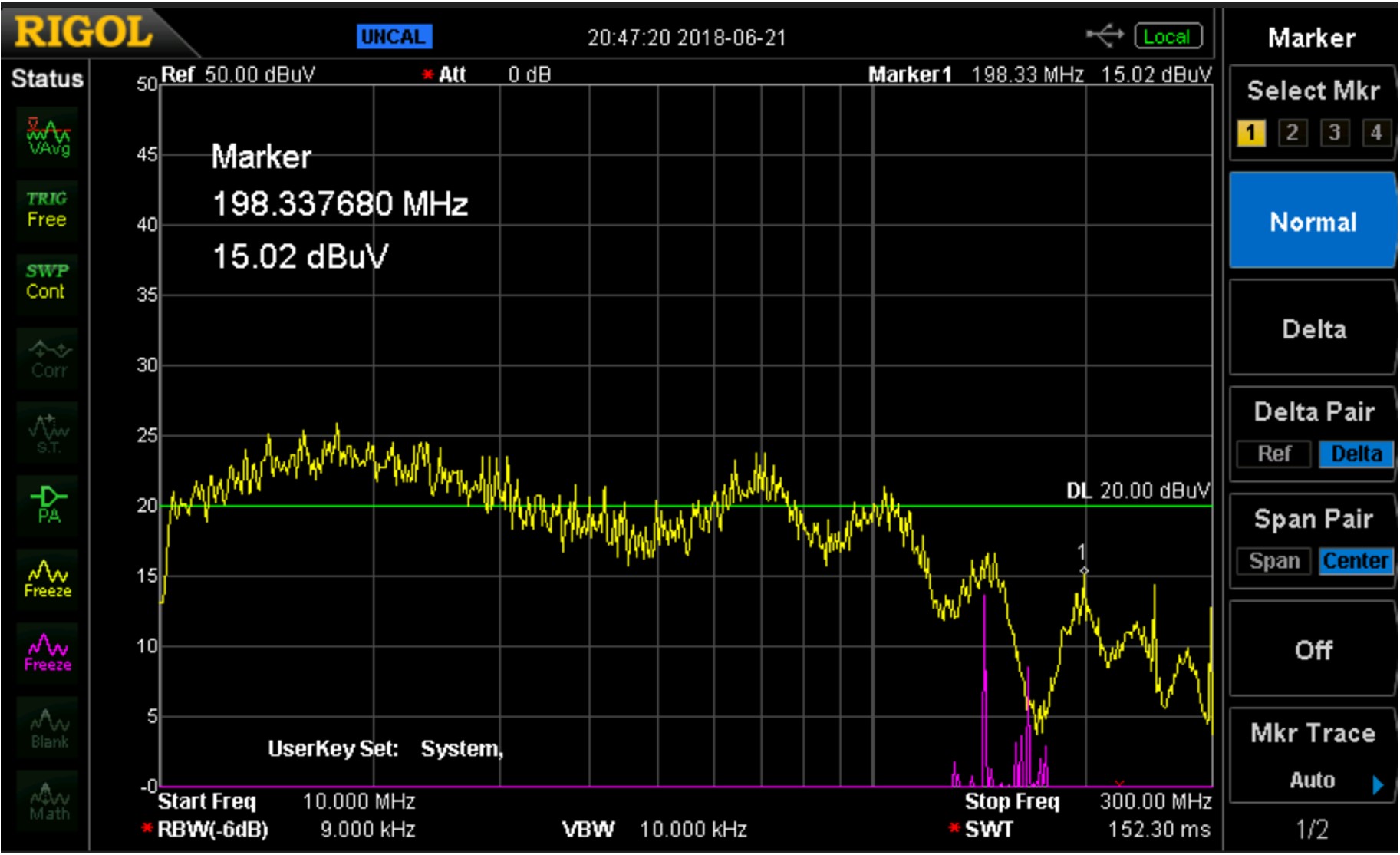 NCP 81239 near-field emissions after fix
UPDATE:
Adding series impedance to decoupling caps has a negative side effect of higher supply bounce. In this case, we decided that we did not want the additional supply bounce and instead isolated the decoupling cap return to minimize noise injection to the general ground planes. In this case, it meant disconnecting the cap return side via from all but the adjacent layer.

By: Dave
Dave is skilled in circuit design, PCB layout, and EMC - specializing in automotive power electronics hardware design. In addition to 10+ years as an electronics consultant, Dave spent his career in the automotive industry from engineering to upper management. Dave is a registered Professional Engineer (Mechanical). He also holds a MS in Computer Science (Laurence Tech 06') and a BS in Mechanical Engineering (GMI 86').
Like what you see?
Experiments
About Us
DEB Associates helps companies through the entire electronics design process. Our team is smart, reliable, and deeply knowledgeable about the intricacies of circuit design, PCB layout, and EMC.
DEB Associates 2020